Printed circuit boards or PCBs are among the most common things you’ll encounter if you’re into electronics. By removing all of the connecting wires and breadboards, these boards help to save time and space. A PCB can efficiently reduce the overall size and weight of the device you’re building. In this article, we will talk about different types of PCBs and how to build one step by step correctly.
There are three main techniques of building PCBs, they include:
- Laser cutting technique(edge etching)
- Connecting circuit by hand on PCB
- Iron on glossy paper technique
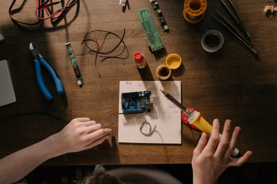
Laser cutting edge etching is mostly used in the large-scale production of PCBs at the industrial level. This step-by-step guide will help you build your first PCB by yourself at home. For materials, you will need an iron box, copper clad laminate, some kitchen scrubs, a laser printer, etching solution, acetone, and some plastic coated wire.
Design and Print Out Your PCB Design
You can use different software to design your PCB schematic diagrams, such as PCB wizard or Autodesk Eagle. If you want a high-quality export after designing your PCB layout, set the DPIG during export to 1200. When printing out your layout, mirror the image of the printout and print it on glossy paper, on the glossy side.
Transfer Your Design Onto a Copper Plate
Next, trim your copper-clad laminate board to your desired size with a cutter, and using the kitchen scrub, scrub the copper side of the plate to remove the top oxide coating on copper.
Iron the Design Onto the PCB Base
Next, you want to transfer your printed PCB design onto the copper board. Flip the printed image horizontally and place it on the copper side of the PCB board. To transfer the image to the board, heat an iron box and place it on the backside of the glossy paper for about 10 seconds. With some little pressure applied, gently iron the glossy paper stuck on the copper plate for about 10 minutes. This will transfer the ink onto the surface of the copper plate.
Etching
After ironing, you can get rid of the paper by soaking the board in some water for a few minutes. To etch the design onto the plate, mix your etching solution(ferric chloride soln) into a plastic container. Now dip your PCB plate into the solution and let it sit for 20 to 30 minutes. The solution will remove the uncoated copper from the board, leaving only your printed design on the plate.
Trimming, Cleaning, and Inspection
Once your etching is complete, carefully dispose of your etching solution by diluting it to reduce the concentration and then pouring it in a safe place(not the sink since it might corrode the pipes). Now all that’s left is to clean your PCB plate with some acetone on a paper towel to remove the printer ink to expose the copper. Now trim your PCB to its final size and then drill your holes onto the board. Your PCB is now ready to be soldered onto and can take components. If you want to provide your PCB for other businesses, you can then work with a printed circuit board shipping company to properly package and ship your PCB.
Printed circuit boards are helpful in many industries right now. If you are interested in learning how to create them on your own, follow the above steps.